Dive into the world of electronics with our comprehensive look at the Ltk5302 Ic Pinout Diagram. Understanding this diagram is crucial for anyone working with this specific integrated circuit, offering a clear roadmap to its functionality and connections.
Decoding the Ltk5302 Ic Pinout Diagram
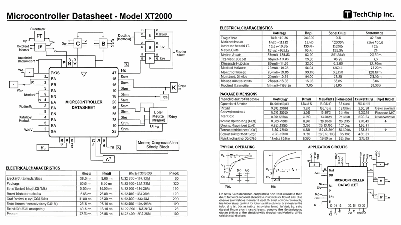
The Ltk5302 Ic Pinout Diagram is essentially a blueprint for a tiny electronic component, an integrated circuit (IC) known as the Ltk5302. Think of it like a map that shows you where each connection point, or "pin," on the chip leads and what its purpose is. Without this diagram, trying to connect the Ltk5302 to other electronic parts would be like navigating a city without a map – confusing and prone to errors. It details the physical layout of the pins and assigns each one a specific function, such as providing power, sending signals, or receiving data.
These diagrams are indispensable tools for engineers, hobbyists, and technicians. They facilitate accurate circuit design and troubleshooting. For instance, when building a new device or repairing an existing one, the Ltk5302 Ic Pinout Diagram helps determine:
- Which pins need to be connected to the power supply.
- Which pins are used for input signals.
- Which pins are used for output signals.
- Any special function pins that control specific operations.
The importance of correctly interpreting the Ltk5302 Ic Pinout Diagram cannot be overstated. Making the wrong connection can lead to a malfunctioning circuit, damage to the IC itself, or even a safety hazard. Therefore, meticulous attention to detail when referencing this diagram is paramount for successful electronic projects.
To further illustrate the typical information found, consider a simplified representation:
| Pin Number | Pin Name | Function |
|---|---|---|
| 1 | VCC | Positive Power Supply |
| 2 | GND | Ground |
| 3 | INPUT_A | First Input Signal |
| 4 | OUTPUT_X | First Output Signal |
As you can see, each pin has a clear role. Understanding these roles allows for precise connections and efficient operation of the Ltk5302 IC in its intended application. For example, you might need to connect Pin 1 to your circuit's positive voltage source and Pin 2 to ground. Then, signals would be routed to or from pins like INPUT_A and OUTPUT_X as required by your circuit's design.
Ready to put your knowledge to practice? Refer to the detailed Ltk5302 Ic Pinout Diagram provided in the section that follows to ensure accurate and effective implementation in your next electronic endeavor.